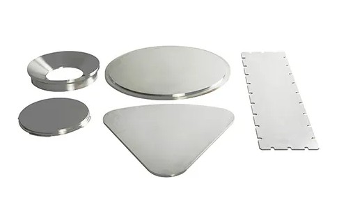
Molybdenum sputtering targets for electrode and wiring materials in flat-panel displays, thin-film solar cells and barrier layers in semiconductors — built on molybdenum's high melting point, high conductivity, low resistivity and good corrosion resistance. Available as rotary and planar targets in pure Mo (Mo-1) and TZM, with tight grain size, roughness and flatness control. All sizes custom to your drawing.
| Type | Dimensions (mm) |
|---|---|
| Rotary target (OD × ID × L) | Φ140 – 180 × Φ125 – 135 × 100 – 3300 |
| Planar — rectangular (L × W × T) | 10 – 3000 × 10 – 800 × 1.0 – 50.8 |
| Planar — round (Ø × T) | Ø10 – 1000 × 1.0 – 100 |
| Composition | Molybdenum (Mo-1 · TZM) |
| Purity | ≥ 99.95% |
| Density | 10.2 g/cm³ |
| Grain size | ≤ 100 µm² (or to requirement) |
| Roughness | Ra ≤ 0.4 µm |
| Flatness tolerance | < 4 µm |
| Standard | ASTM B386 |
| Atomic number | 42 |
| CAS number | 7439-98-7 |
| Atomic mass | 95.94 g/mol |
| Melting point | 2620 °C |
| Boiling point | 4639 °C |
| Density (20 °C) | 10.22 g/cm³ |
| Crystal structure | Body-centered cubic |
| Thermal expansion (20 °C) | 5.2 × 10⁻⁶ m/(m·K) |
| Thermal conductivity (20 °C) | 142 W/(m·K) |
| Specific heat (20 °C) | 0.25 J/(g·K) |
| Electrical conductivity (20 °C) | 17.9 × 10⁶ S/m |
| Resistivity (20 °C) | 0.056 (Ω·mm²)/m |
Mo powder mixed to grade.
Cold isostatic pressing.
Medium-frequency sintering furnace.
Machined and finished to roughness / flatness spec.
Electrode and wiring material for FPD and TFT-LCD.
Back-contact and electrode layers for thin-film PV.
Barrier-layer material for semiconductor devices.
Targets for sensors, FED and functional thin films.
Send your target type (rotary / planar), dimensions and grade (Mo / TZM) — or a drawing. Quotes within one business day.